IC footprint
Published on 1/3/2017 10:53:35 AM
Description
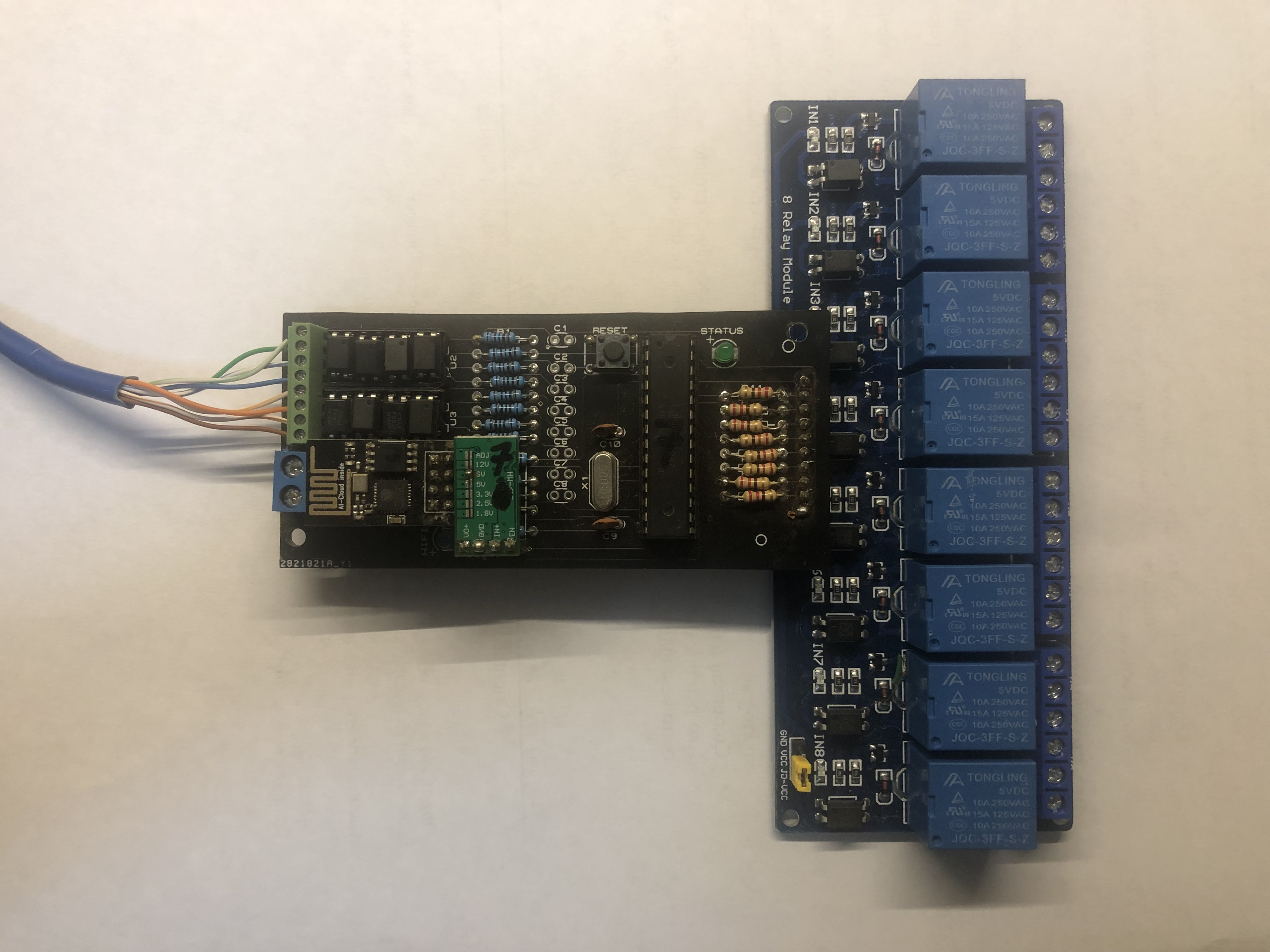
I have a problem with the layout of an dip socket.<br /> I toke the housings_DIP:DIP-14_W7.62mm footprint.<br /> but every time I open the PCB it makes pin 7 and 14 GND.<br /> while the pin 14 should be VCC.<br /> <br /> If I show up the invicable pins in the schematic, then it is labeled correct.<br /> As you can see on the pictures it labels pin 7 & 14 gnd and connects them together<br /> I also have some header pins in the schematic.<br /> VCC and GND should be connect to the headers.<br /> <img src="https://file.allpcb.com/bbs/17/01/03/105330106.jpg" alt="" /><br /> Who is able to help me?<br />
28
comment
All comments
 Unknown
5247
0
28
Rules about cashback: 1. Valid time: ALLPCB cashback activity will end on April 1st. 2. Capped amount: The capped amount of cashback for each account is $5,000. Each order can get a maximum of $2,000 cashback. That means every author can get $5,000 max. 3. Cashback range: The cashback activity only covers the corresponding PCB order. The order amount for other combined payment products will be invalid. 4. Clicking your own promotional link will be invalid. The same email address, shipping address, contact information, and phone number are all recognized as the same account. 5. ALLPCB has the final interpretation right of the cashback activity.
ALLPCB will donate 2% to the author for this promotion link.

